

What Is The Process Of Installing A High—Performance Electron-Beam Lithography System?
The high-performance electron beam lithography systems feature fully automated and cost-effective systems designed for industrial applications and advanced research. Therefore, the high-performance electron lithography system is ideal for application in areas where the throughput and precision are critical.
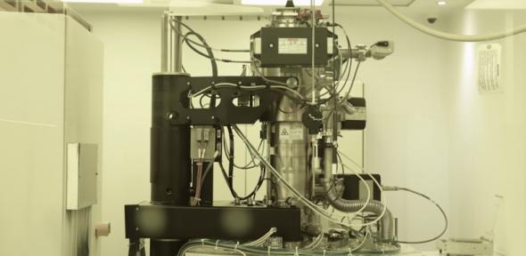
To understand the installation procedure, we look at the basic construction of the Electron Beam Lithography System. A typical EBL system comprises of the following components:
- Electron source
- Electron column for shaping and focusing the beam
- A mechanical stage for positioning wafer under the electron beam
- Wafer handling mechanism that automatically loads and unloads the wafer
- A computerized system that controls the equipment
- A vacuum system is needed to maintain appropriate vacuum level throughput and prevent the electronics supplies power and signals to various parts of the machine.
While installing the electron beam lithography system, ensure the electron gun, the beam’s source is positioned at the column’s top. Note that electron lithography systems feature two types of electron guns. These are the thermionic and field emissions.
The electron beam lithography forms the electron beam commonly referred to as the column. The column features the electron source, two or more lenses, and a mechanism for deflecting the beam.
Now that you know the high-performance electron beam lithography system components and how the systems work, we analyze two popular systems, the VOYAGER™ and Vistec’s SB254.
VOYAGER™
This is a dedicated high-performance electron beam lithography system commonly used in academics and for industrial applications. The VOYAGER™ is mainly known to ensure high throughput and precision. Based on the Raiths smart and innovative eWrite technology, the electron lithography system is designed from scratch for those looking for a super-fast turnover and those in need of small-batch technology with a reliable and economical workhorse.
The high-performance system is easy to use and features reasonable pricing while the performance is high throughout the instrument’s lifetime. Besides, the VOYAGER™ electron beam lithography system features an environment-tolerant shield ensuring system stability. Here is an overview of the features you get with this High-Performance Electron-beam Lithography System:
- Features 50 kV thermal field emission column technology
- Has a fully-automated write field calibration
- Based on an automatic focus and stigmator setup
- A mechanical switch between the high-resolution and throughput writing mode
- Multiple sample exposure automation
- Compact system footprint
The high-performance system features Innovative, upgradable, and future-proof system architecture. It is available at attractive pricing, while the throughput and precision are high rated.
Vistec’s SB254
Vistec’s SB254 is a fully automated and high-performance electron beam lithography system designed for application in industrial and advanced research application cases.
The high performance and cost-effective lithography system feature a reliable and field-proven design based on the Variable Shaped Beam (VSB) principle. Vistec’s SB254 is utilized in a wide range of existing and emerging semiconductor and nanotechnology applications. The application areas include silicon direct write, silicon photonics, compound semiconductor, mask making, and integrated optics. Vistec’s SB254 is a reliable, field-proven system that ensures a high throughput rate suitable for 24/7 production environments. The unit features numerous worldwide installations supported by an efficient international service organization.
Key Features of the Vistec’s SB254:
- Comes with a wide range of substrate sizes and types
- Has a substrate material covering a wide variety of all commonly used materials
- Built with the mark detection software package for mix and match
- Delivers a high accuracy field with keystone correction
- Features Multipass writing and comes with substrate edge detection
The Electron beam lithography systems feature a specialized technique that creates fine prints much smaller than can be seen by the naked eye. The main attribute of the electron beam lithography technology is its capability to ensure a very high resolution.
The technology works with a variety of materials and an almost infinite number of patterns. Currently, the electron beam lithography technology is used in the integrated circuit industry where high-performance electron beam lithography systems are required.